Physical Address
304 North Cardinal St.
Dorchester Center, MA 02124
Physical Address
304 North Cardinal St.
Dorchester Center, MA 02124

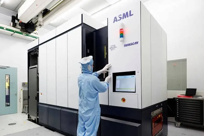
Dutch semiconductor equipment manufacturer ASML has announced plans to work with some of the world’s biggest chipmakers to adapt its latest lithography technology for producing larger and more powerful chips used in advanced data centres.
ASML, one of the leading suppliers of chipmaking equipment, produces lithography machines that use light to transfer intricate circuit patterns onto silicon wafers.
Its existing extreme ultraviolet (EUV) machines are capable of producing chips measuring up to roughly 800 square millimetres.
Major technology companies, including Nvidia and Google, are already designing increasingly sophisticated processors that approach this size limit as demand for artificial intelligence and data-centre computing continues to grow.
ASML’s next-generation machines, known as High-NA EUV systems, are designed to create even smaller and more precise features on chips.
However, the machines currently face a limitation because they use smaller masks, which restrict the maximum size of chips that can be produced.
The company said it plans to work with major customers on developing larger masks for its High-NA machines.
The change would allow the technology to manufacture chips that are comparable in size to some of the largest processors currently used in data centres.
ASML believes the larger masks could help accelerate the adoption of High-NA EUV technology for large-scale chip production.
The latest machines are already being used by Intel for production, but Taiwan Semiconductor Manufacturing Company (TSMC) and Samsung Electronics have yet to deploy them for high-volume manufacturing.
South Korean memory-chip maker SK Hynix also said it is considering joining the industry consortium working on the introduction of 12-inch masks.
The company is targeting 2028 for the use of High-NA EUV technology in mass production of DRAM memory chips.
TSMC has said it intends to introduce ASML’s High-NA technology into high-volume production of advanced-node chips from 2030.
Samsung, meanwhile, is planning to use High-NA EUV for high-volume DRAM production by 2028.
ASML expects to demonstrate a pilot production line using the larger masks by 2031, with the technology potentially becoming ready for high-volume manufacturing by 2033.
The company believes the development could significantly improve the productivity of High-NA systems.
ASML Chief Technology Officer Marco Pieters said industry-wide adoption of the larger-mask technology could increase the productivity of the machines by about 40 percent.
The planned development highlights the semiconductor industry’s efforts to produce increasingly powerful processors as demand for artificial intelligence, cloud computing and data-centre infrastructure continues to rise.
Join us on our WhatsApp Platform @KOIKIMEDIA NEWS YOUR PAGE
Koikimedia Bringing the World 🌎 Closer to Your Doorstep

[mc4wp_form id=2402]